
Attention at the Power Cap: a Fast bf16 Attention Kernel for CDNA4
A bf16 forward attention kernel for CDNA4, written in HIP, that is 1.08–1.15× faster than AITER's hand-tuned v4 assembly on dense shapes and 1.16–1.19× faster than AITER's fastest causal kernel. It runs about the same number of cycles as v4; the difference is a 12–13% higher clock under the same 1400 W cap.
TL;DR
- A bf16 forward attention kernel for CDNA4, head dimension 128, written in HIP.
- On this chip a plain matrix stream already hits the 1400 W cap, so the kernel is built to use less energy per FLOP.
- Two waves share each SIMD: while one runs matrix instructions, the other runs its softmax in the gaps. We cut the softmax down to two vector instructions per matrix instruction, so it hides completely behind the matrix work.
- That lets us use 16×16×32, which draws 12–16% less power per FLOP than the default 32×32×16.
- About the same cycle count as AITER's hand-written v4, at a 12–13% higher clock: 1.08–1.15× faster on dense shapes, 1.16–1.19× on causal ones.
- The CDNA4 attention code is open source under the MIT license.
1. What we built, and the idea behind it
This is the CDNA4 follow-up to our MI300X attention kernel. It is a full bf16 forward attention kernel for CDNA4 with head dimension 128: dense and causal, grouped-query attention, variable-length and paged KV, and an optional log-sum-exp output.
We started the way we did on CDNA3, by taking the fastest existing kernel apart. AITER's v4 forward attention is hand-written assembly, and by our counter measurements it keeps the matrix core about 97% busy inside its main loop. On CDNA3 we won by planning the schedule better than the compiler would. On CDNA4 there was very little schedule left to win.
So we looked at power instead. On MI355X, a plain stream of matrix instructions is enough to hold the card at its 1400 W cap. At the cap, the clock is set by how much energy the work burns, so a kernel that spends fewer joules per FLOP can run at a higher clock. That is the idea behind every design decision in this post: the matrix instruction (§3.2), the softmax (§3.3), and the tile size (§4.2).
The post is structured as follows. §2 explains why the power cap changes what counts as an optimization. §3 covers the architecture: the wave schedule, the matrix instruction, and the softmax built to fit it. §4 covers the memory layout. The results are in §5.
2. Optimizing at the power cap
A stream of v_mfma instructions with changing operands, eight waves per CU, settles at 1700–1890 MHz on MI355X. A lighter one-SIMD-per-CU stream reaches ~2400 MHz (the top clock) at ~710 W. The difference is power: the full stream draws ~1320 W, and the card lowers its clock until it stays there. Attention adds softmax, LDS traffic, and memory traffic on top of the matrix work, so attention kernels on this chip run at the cap too.
With the power fixed, a kernel's time is roughly its energy divided by 1400 W. That has a consequence we had to learn by measuring. Removing idle cycles helps much less than it looks, because the same work still costs the same joules, and the clock drops to keep the power at the cap. When we added pure idle cycles to our kernel, every 1% of extra cycles cost only 0.4–0.5% of time. Removing energy is what moves the time: the clock rises and the same work finishes sooner.
So the number we optimized was energy per FLOP, measured as time at the cap. Cycle counts still matter for diagnosis, but a change that saves cycles and burns the same energy is mostly a wash.
3. The architecture
3.1 Eight waves, two groups, one barrier per tile
The structure is the one we used on CDNA3. A workgroup has eight waves, two per SIMD, in two groups of four. Waves w and w + 4 share a SIMD. For each 64-key tile, a wave runs a matrix block, S(t) = Q·K(t)ᵀ and O += P(t−1)·V(t−1), then a softmax that turns S(t) into P(t). Group A runs half a tile ahead of group B, so on every SIMD one wave is in its matrix block while the other is in its softmax.
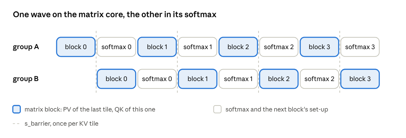
Between two barriers, group A runs a softmax and then a matrix block, and group B does the opposite. The softmax's VALU instructions issue in the gaps the partner's matrix instructions leave.
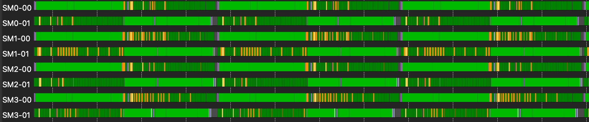
Two things changed from CDNA3. The first is synchronization. The CDNA3 kernel needed two barriers per iteration. Here each group runs its own copy of the loop, with the group fixed at compile time, and the differences between the groups (which tiles each loads ahead, where its barrier sits, its issue priority) are constants in that copy. That leaves one s_barrier per KV tile.
The second is that K and V both go through LDS. On CDNA4 the direct-to-LDS load, buffer_load_dwordx4 … lds, moves 16 bytes per lane, and LDS is 160 KiB per CU, so K and V each get a three-deep ring of tiles. Every wave loads its own 8-row slab of each tile, so the loads are spread across all eight waves and issued inside the matrix block, behind the MFMAs.
3.2 Why 16×16×32, not 32×32×16
On paper, v_mfma_f32_32x32x16_bf16 is the default choice for attention on CDNA4, and AITER's assembly uses it. It does twice the FLOPs per instruction and occupies the matrix core for 32 cycles, while blocking the partner wave's VALU for only 8 of them. That leaves room for 6 VALU instructions beside every MFMA, plenty for a softmax.
v_mfma_f32_16x16x32_bf16 is more efficient, if the kernel has room for it. Its accumulator is 4 registers per lane instead of 16, so for the same FLOPs it reads and writes half the accumulator values. That shows up as power. Two pure matrix streams with the same FLOPs at the cap ran 1888 TF/s at 1893 MHz with 16×16×32 and 1681 TF/s at 1699 MHz with 32×32×16. At a locked clock, the 16×16×32 stream drew 12–16% less power.
It also has a structural payoff, the same one as on CDNA3. A 16-row tile lets a wave hold three query tiles, 48 rows. With 32×32 tiles the choice is 32 or 64 rows, and 64 does not fit the register file. §4.2 covers why the extra rows matter.
The cost is issue room. A 16×16×32 MFMA takes 16 cycles and blocks the VALU of both waves on the SIMD for the first 8, which leaves 2 VALU slots per instruction, a third less room per FLOP. An exponential needs both slots.
3.3 Fitting the softmax beside 16×16×32
The softmax of one wave has to fit in the time its partner spends on a matrix block: 96 MFMAs and 3 row-sum instructions, 1584 cycles. Two limits apply at once. A wave issues at most one instruction every 4 cycles, which gives 396 issue slots for everything. And the VALU is blocked for 8 cycles after each MFMA and 12 after each row-sum instruction, which leaves 195 of those slots for VALU. Scalar, LDS and branch instructions are not blocked, so they can use the cycles right after an MFMA, which the VALU cannot.
Some softmax work cannot be avoided. Every score needs one multiply by the softmax scale, one exponential, its share of the row maximum, and its share of the pack to bf16. With 48 scores per lane per tile, that alone fills the VALU budget:
| Softmax wave, per KV tile | Needed | Available |
|---|---|---|
| VALU slots | 196 | 195 |
| All issue slots | 250 | 396 |
What fills them:
- 195 VALU slots available: a 16×16×32 MFMA blocks VALU issue for 8 of its 16 cycles, leaving 2 slots each (96 × 2 = 192); a row-sum smfmac blocks 12, leaving 1 each (3 × 1 = 3).
- 196 VALU slots used: 48 exponentials at 2 slots each (96), 48 multiplies by the softmax scale, 25 row-maximum instructions (three scores each), 24 bf16 packs (two scores each), 2 adds that put the next block's LDS offsets on each lane's base address, and 1 compare for the rescale test.
- 54 non-VALU slots used, of 396 total: 40 scalar instructions (the next block's load and address set-up, combining the rescale test across the wave, loop control), 3 row-sum instructions, 4 LDS reads, 4 branches, 2 waits and 1 barrier.
Total issue has room to spare. The VALU does not: it is exactly full.
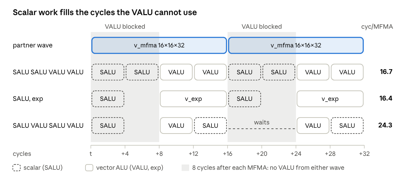
Two scalar instructions plus two back-to-back VALU fit in one MFMA window, and so do a scalar instruction and an exponential. A scalar instruction placed between the two VALU pushes the second one into the next window.
So the softmax wave can only run at full speed if about half of what it issues is not VALU, and its VALU stays in back-to-back pairs or single exponentials. Anything that is the same for every lane of a wave should be a scalar instruction: on the VALU it would take a slot the exponentials need, and on the scalar unit it fills a cycle the VALU cannot use. This is what we moved to scalar instructions:
- The ring-buffer slot of the next K and V tiles (tile index mod 3, done with a multiply, not a divide).
- The next block's load set-up: source byte offsets of K and V, LDS destinations, and
M0. - The LDS read bases of the next block. Each lane adds them to one base register it keeps for the whole kernel, two VALU adds per tile.
- The rescale decision. The per-lane compare is one VALU instruction; combining it across the wave and branching is scalar.
- The check for rare tiles (first tile, masked edge tiles), one scalar compare against the next rare tile's index, and the loop counter.
So everything else had to come off the common tile, or off the VALU. Five decisions did it.
- A lazy rescale with a lane-local test. Each row keeps a reference maximum that only moves when the row's maximum passes it by 8 in log2 units, so the largest unnormalized probability is 2^8, the bound FlyDSL and the Triton gluon tutorial kernel use. When it moves, it jumps 16 above the new maximum. Each lane compares its own partial maxima with the threshold, and one wave-wide ballot decides whether any row needs a rescale, so a common tile never combines a row maximum across lanes. The rescale of O and the row sums runs out of line, on about 1% of tiles or fewer on real model activations.
- Rare tiles out of line. Masking for the edge tiles of a sequence or a causal diagonal, the first tile's set-up and the occasional buffer-resource move all sit behind one scalar compare per tile. Interior tiles skip them with a single branch.
- Row sums on the matrix core. A sparse
v_smfmac_f32_16x16x64_bf16with a 2:4-sparse A operand of ones sums two P fragments per instruction, three instructions per tile. Summing on the VALU would cost one add per score, 48 more slots, a quarter over budget. - Per-tile work on the scalar unit. Everything listed above. Packed fp32 instructions (
v_pk_*_f32) also get no issue slot beside an MFMA, so the kernel is built with-fno-slp-vectorizeto stop the compiler from forming them. - The order of the work. The softmax runs in three fenced phases: the multiplies and the maximum, then the exponentials with the scalar set-up interleaved between them, then the packs. That keeps each exponential at the start of a window and the scalar instructions in blocked cycles.
softmax(tile t):
  if (t is a rare tile) handle_rare_tile(t)        // first tile, masked edge tiles: out of line
  1. s *= scale; lane max vs threshold; one ballot  // multiplies and max
     if (ballot) rescale()                          // about 1% of tiles, out of line
  2. p = exp2(s), back to back                      // next block's scalar set-up in between
  3. pack p to bf16                                 // P for the next block's PV
With the VALU exactly full, every VALU instruction we added later had to pay for itself. That budget is the reason the kernel can use the more efficient instruction.
4. The memory layout
4.1 What lives where
MI355X has 256 CUs, each with 160 KiB of LDS. The kernel uses all 256 VGPRs a wave can address, with no AGPRs and no spills, and 141 KiB of LDS:
| Data | Lives in | Why |
|---|---|---|
Q tiles 0 and 1 | VGPRs, loaded once | QK's B operand on every step. |
Q tile 2 | LDS, one slot per wave | No room for all of it in registers. Read one 32-wide k-step at a time, 4 reads per KV tile; each piece feeds 4 MFMAs, so only 4 VGPRs of it are live instead of 16. |
K, V tiles | LDS, three-deep rings, direct DMA | Each tile is shared by all eight waves; never passes through VGPRs. |
S, O | VGPRs, fp32, transposed | With q on the MFMA's N axis, a row's softmax stays in one lane. |
P | VGPRs, bf16 | PV's B operand, packed straight from the exponentials. |
S and O are held transposed, as on CDNA3, so each lane owns whole query rows. On a common tile the softmax has no cross-lane step at all: each lane checks its own partial maxima against the threshold, and one wave-wide ballot decides whether any row needs a rescale.
4.2 Wider tiles, more reuse per byte
AITER v4 gives each workgroup 256 query rows, 32 per wave. We give each workgroup 384 rows, 48 per wave. Every K and V byte that arrives from L2 serves 1.5× as many query rows, so the kernel moves a third fewer K and V bytes per FLOP. Inside the workgroup, each K or V fragment a wave reads from LDS feeds three matrix instructions instead of two:
| Per wave, per 64-key tile | AITER v4 | Ours |
|---|---|---|
| Query rows | 32 | 48 |
| LDS bytes read per lane (K, V, and our third Q tile) | 512 | 576 |
| LDS bytes per lane, per query row | 16 | 12 |
Fewer bytes moved per FLOP is the one optimization where energy and cycles point the same way.
4.3 V is transposed in the read
On CDNA3, V needed a separate transpose kernel (§4.4 of the CDNA3 post), because the PV matmul wants V with keys along the reduction dimension. CDNA4 adds ds_read_b64_tr_b16, which transposes 16-bit elements as it reads them from LDS. Two of them form one V operand, so V is stored in LDS as it arrives from memory and the extra kernel is gone. K uses plain ds_read_b128 with an XOR swizzle on the row's 16-byte chunks, and the pitches are chosen so every 16-lane read pass hits distinct banks. The hardware counter for LDS bank conflicts reads zero.
5. Results and takeaways
Measured on MI355X (gfx950, 1400 W cap), bf16, head dimension 128. Every kernel runs in rotated 250 ms blocks, alternating direction each round, with the last-level cache flushed before every block; the first four rounds are discarded and the median of the next twelve is reported. Every kernel's output is checked against an fp32 reference on sampled rows before it is timed. The baselines are AITER's kernels from release v0.1.25: the v4 and v3 assembly kernels and the HIP opus kernel. AITER v4 has no causal variant. Speedup is aiter_ms / ours_ms against the fastest AITER kernel on that shape. The small-grid row fills only part of the GPU.
| Shape (B, H, S, D) | Ours (ms) | AITER v4 (ms) | AITER v3 (ms) | AITER opus (ms) | Speedup |
|---|---|---|---|---|---|
| (16, 16, 16384, 128) dense | 22.466 | 25.812 | 27.992 | 26.101 | 1.15× |
| (32, 8, 8192, 128) dense | 5.773 | 6.407 | 6.981 | 6.609 | 1.11× |
| (8, 16, 4096, 128) dense | 0.788 | 0.850 | 0.917 | 0.851 | 1.08× |
| (2, 32, 32768, 128) dense | 22.534 | 25.851 | 28.006 | 28.368 | 1.15× |
| (4, 64/8, 8192, 128) GQA dense | 5.725 | 6.517 | 7.068 | 6.628 | 1.14× |
| (16, 16, 16384, 128) causal | 11.859 | – | 14.291 | 14.161 | 1.19× |
| (4, 64/8, 8192, 128) GQA causal | 2.948 | – | 3.679 | 3.480 | 1.18× |
| (1, 32/8, 65536, 128) GQA causal | 22.402 | – | 28.157 | 26.154 | 1.17× |
| (8, 32/8, 4096, 128) GQA causal | 0.814 | – | 0.998 | 0.947 | 1.16× |
| (1, 8/1, 4096, 128) causal, small grid | 0.052 | – | 0.084 | 0.068 | 1.30× |
The dense rows show where the speed comes from. Clock is the median gfx clock sampled during each kernel's blocks; cycles are time multiplied by that clock, so they are estimates.
| Shape, against AITER v4 | Clock, ours | Clock, v4 | Cycles, ours / v4 | Time, ours / v4 |
|---|---|---|---|---|
| (16, 16, 16384, 128) dense | 1731 MHz | 1541 MHz | 0.98 | 0.87 |
| (32, 8, 8192, 128) dense | 1756 MHz | 1553 MHz | 1.02 | 0.90 |
The two kernels need about the same number of cycles. Ours runs them at a 12–13% higher clock, because at the same 1400 W it spends less energy on each one.
What we would take away:
- On a power-capped GPU, optimize energy per FLOP. Removing cycles that do not burn energy mostly lowers the clock. Removing energy raises it.
- Fit the softmax to the instruction you want. 16×16×32 leaves two VALU slots per instruction. A lazy, lane-local rescale test, rare tiles out of line, row sums on the matrix core and no VALU bookkeeping bring the softmax inside that budget.
- 32×32×16 is the default on paper; 16×16×32 is better when it fits. It does the same work with half the accumulator traffic and 12–16% less power, and its 16-row tiles let a wave hold 48 rows.
- The structure carried over from CDNA3. Eight waves, two groups, transposed S and O, three Q tiles per wave. CDNA4's direct-to-LDS loads and transposing LDS reads made it simpler: one barrier per tile and no V transpose kernel.
The code is available at github.com/moonmath-ai/amd-kernels